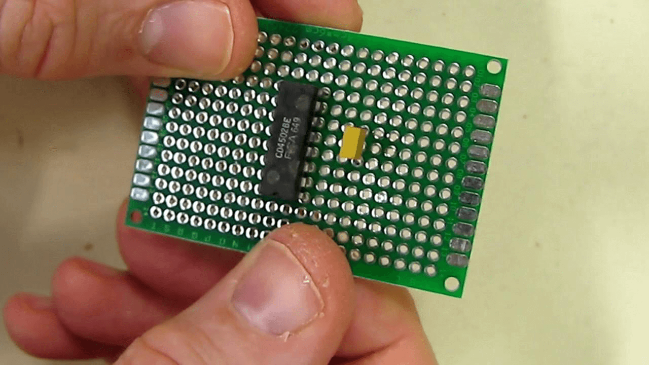
HDI High-Density Interconnect PCB Printed Circuit Board
HDI PCBs are very common these days. It is a type of Printed Circuit Board (PCB) used in electronic devices. HDI is an abbreviation for high-density Interconnect. In this article, I am going to tell you all about HDI PCB.
HDI PCB Overview
HDI is a sort of PCB with high wiring density per unit area as compared to a typically printed circuit board (PCB). Simply, HDI PCB is described as the PCB with a single of all the following characters:
- Microvias
- Blind and buried vias
- Build-up lamination
- High signal concern
PCB technology has been going through many phases. PCBs are evolved from big sizes to very small sizes and faster speeds with HDI technology. HDI is a type of PCB but in small having smaller vias, and pads as compared to a typical PCB. Technology evolved the PCB to a lighter weight and compact size. Instead of using many PCBs as a single device, one HDI PCB Manufacturer can handle the entire functionality of the boards.
Advantages of HDI PCBs
HDI PCB is the latest evolution in PCB. HDI PCBs are smaller and more efficient as compared to a typical PCB. The major advantage of HDI PCBs is that they can function more with less. The copper-etching technology enabled it to be refined for better accuracy. Technology makes it possible to enable one HDI PCB to hold the functionalities of multiple PCBs.
It reduces the distance between the device and the trace place. It enables the HDI PCB manufacturers to organize a wide number of transistors to get better performance in electronic devices while reducing power consumption. Signal reliability is also enhanced in HDI due to the small distant connections and low power consumption. Other things that are enhanced in the PCB with HDI technology are stable voltage rail, closer ground, and much more.
Some of the major advantages of HDI PCBs are highlighted below:
HDI PCBs are cost-friendly: HDI are properly planned so, they reduce the overall cost due to the number of essential layers, small size, few numbers of required boards, and lower power consumption.
Faster Time-to-Market: HDI PCB manufacturers are capable of fastly marketing the product if they built the design with proper planning. It also happened due to the easy organization of components and enhanced performance. It takes short time to test the HDI PCB.
Enhanced Reliability: HDI PCB is much more reliable as compared to the typical PCB because their size is too small and the components are assembled perfectly on the boards.
Common Use of HDI PCBs
HDI PCBs are commonly found in complex electronic devices that need high performance but smaller space. They are used in mobile phones, laptops, computers, touch-screen devices, cameras, 4G and 5G communication networks, and military apps like smart munitions. Want to know more visit Mad PCB
It is also widely used in automotive and aerospace industries where lightweight means more high performance. Cars are becoming more connected and automated using HDI PCBs. Modern cars have 50 microprocessors on the board, which plays a vital role in engine control, safety features, and diagnostics.
